- +86 150 2418 8946
- [email protected]
- +86 15024188946
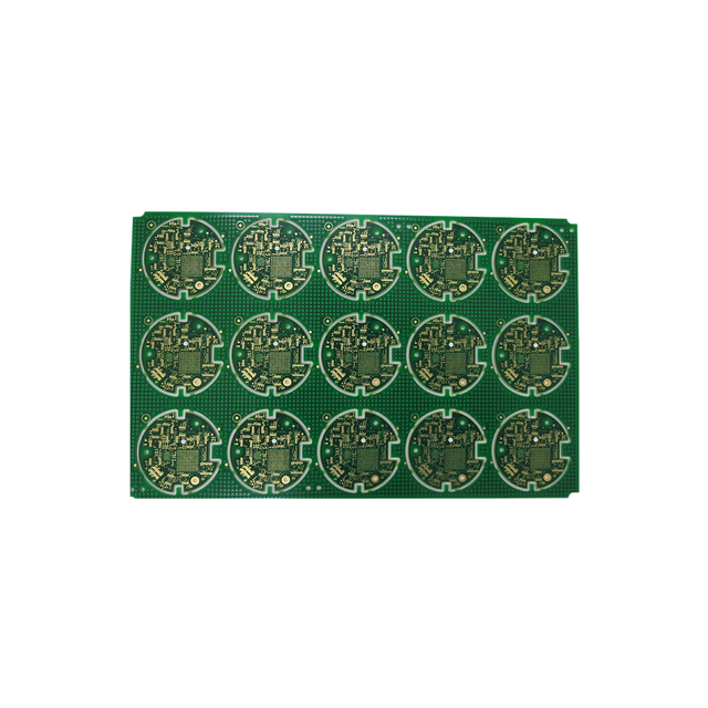
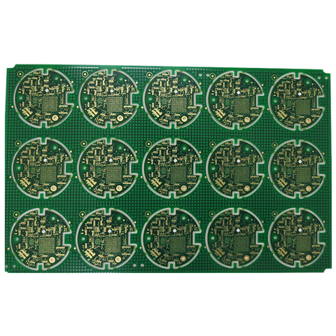
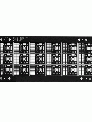
Base Material: KB6167(Tg170)
Copper thickness: 0.5 oz inners,1 oz finish outers,
Board thickness:1.8 mm+/-10%
Solder-mask color: LPI green
Legend color:White
Surface Finish:ENIG(2U”)(Immersion Gold)
Min.vias:0.2mm;
Buried vias:0.2 mm
Min.Track w/d:6/6 mil
Impedance control:+/-10%
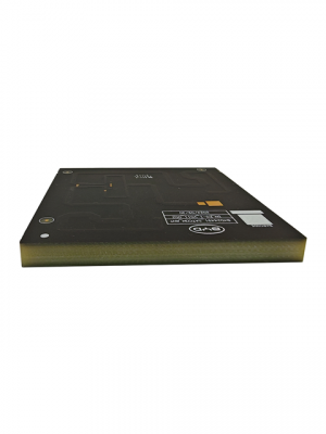
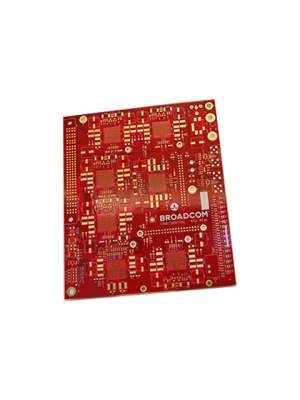
High Density Interconnect(HDI) PCB
High Density Interconnect(HDI) is the printed circuit board with a higher wiring density per unit area than traditional printed circuit boards (PCB). In general, HDI PCBs are defined as PCBs with one or all of the following: microtraces, VIP (Via In Pad), microvias, blind vias, buried vias or other microvia technique, built-up laminations and high signal performance considerations.
Dihe Electronics capabilities of HDI printed circuit boards:
Max. Layer: 30 Layers
Material :FR-4(Normal to High Tg280),Halogen-free, High CTI,ISOLA, Rogers, Teflon,Taconic,Metal Base(Copper/Aluminum/Stainless Steel/Iron)
Min Trace Width/Space:3/3mil
Min hole size:0.1mm
Impedance Control Tolerance:+/-10%
Max. Copper Weight (Inner/Outer Layer): 12.0 oz
Max.Board Thickness: 10.0 mm
Max. Aspect Ratio: 15:1
Surface Finish: HAL Leaded, HAL Leadfree, ENIG(Immersion Gold),Immersion Tin(Chem. Tin), OSP,Gold Finger, Immersion Silver(Ag), Hard gold plating,ENIG+OSP,HAL+Hard gold fingers

